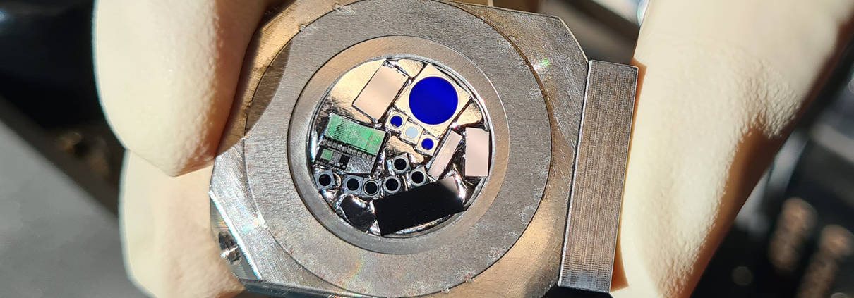
Cameca IMS 7f-Auto (Cameca / Ametek, Inc.)
Secondary ion mass spectrometry SIMS is a solid-state analytical technique for measuring three-dimensional elemental distributions, primarily in the trace and ultratrace range. By bombarding a sample with primary ions (O2+, O- or Cs+) in ultra-high vacuum, secondary ions are released from it (so-called sputtering), which are accelerated in an electric field and, after mass separation, counted in a magnetic field by means of highly sensitive detectors (electron multiplier or low-noise Faraday cup). Vertical information is obtained by sputtering in depth and digital acquisition of count rates of secondary ions over the time axis. Depth resolution reaches values of < 2 nm/decade. Lateral information is obtained by rastering a finely focused primary ion beam over the sample surface and position-dependent signal processing. Elemental distributions can be analyzed three-dimensionally on a micrometer scale with highest detection sensitivity (e.g. boron in silicon from E13 at/cm³). SIMS is a universal measuring method with which, in principle, all elements of the periodic table including their isotopes can be detected qualitatively. Comparison standards are used for quantitative evaluation. The detection limits extend into the range < 1 ppb (1 in 1,000,000,000, for silicon this means a concentration of < 5E+13 at/cm³) with sample volumes in the range 10 µm³. SIMS is therefore an unrivaled analytical tool, especially for research and development tasks in many fields! Typical tasks for SIMS are for example in
- Semiconductor research and manufacturing
and include, among others, the determination of:- Element distributions in one, two and three dimensions
- Doping profiles, penetration depths and concentrations of dopants
- Surface impurities
- Layer sequences, also in non-conducting samples
- Diffusion lengths and constants of doping elements for simulation purposes,
- Segregation within metallization layers,
- Composition and layer thicknesses of insulator layer sequences
- Barrier layers and their effect
- as well as investigations in relation to:
- Adhesion of bonds (e.g. silicon-silicon wafer bonding, hydrophilic/hydrophobic)
- Adhesion of bonds, electroplated layer deposition and soldering
- Foreign sample analysis
- Photovoltaics
- Defect analysis
- Process monitoring
- Optics and glasses
- Surface coatings (e.g. lenses)
- Reflective and anti-reflective coatings
- Filter layers (bandpass filters, UV-VIS-IR filters)
- Aging of surfaces, diffusion of network transducers and leaching processes in glasses
In addition, there are numerous special applications of SIMS in the fields of metallurgy, metal processing (corrosion, surface treatment, decorative and protective coatings, adhesion promoters, …), geology (mass spectra, proof of origin, extraterrestrial material, …) and life science (surface treatment, residual coatings, dental fluoridation, …) or environmental protection (e.g. uranium and its decay products).
Recorded depth profiles of boron in silicon over a certain depth range
Layer analysis for an optical component: The thickness as well as the sequence and number of successive SiO2/SiNx layers were checked. Although this is electrically insulating material, the layer structure could be analyzed down to a depth of 10 µm
Concentration determination of implanted N of mass 14 in diamond: Since nitrogen cannot be detected as a pure N ion, N-C cluster ions have to be analyzed. However, different isotopes interfere here due to the same nominal mass. Thus, at mass 26, 14N12C- (26.0031 amu) interferes with 13C2– (26.0067 amu), 13C12C1H- (26.0112 amu), and 12C21H2– (26.0140 amu). In order to meaningfully quantify nitrogen, mass high-resolution is used to cleanly separate and quantify the individual ions of nearly equal mass


