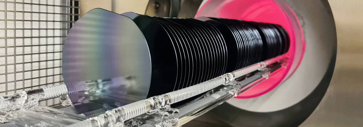
The CiS Research Institute has a range of typical processes for the monolithic integration of sensory and electronic functions in silicon. In a modern clean room, wafers made of silicon and other materials are processed on a dedicated semiconductor production line. Here, various standard processes can be freely combined with additional modules for double-sided and three-dimensional microstructuring of silicon wafers and for the deposition of various functional layers.
On this basis, specific product-independent technology platforms are developed according to the respective requirements. A large number of micro- and nanotechnological technology platforms have already been technologically tested for the production of sensor chips and are available for customer-specific developments, prototyping and small series production. In accordance with the conditions of quality management, process monitoring and documentation are established. In addition to classical test methods, in-house available semiconductor analysis methods, special test methods as well as optical and electrical measurement methods are used.
Under industrial conditions, customer-specific micromechanical and optoelectronic components as well as three-dimensional sensory systems can be developed and realized, including highly specialized photodiodes and photodiode arrays for electron detection and optoelectronic conversion applications in the frequency range from ultraviolet to infrared, piezoresistive strain gauges and pressure sensors.


