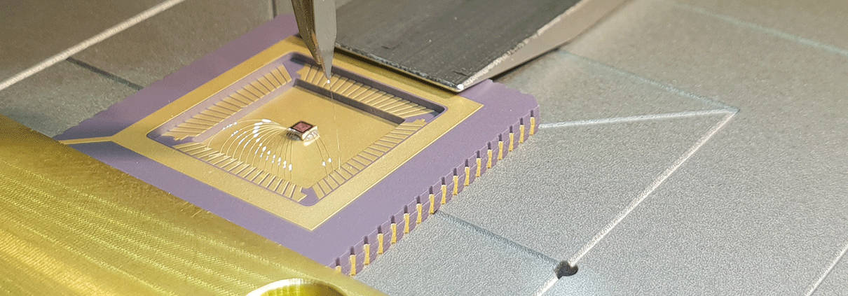
Assembly & Packaging occupies a key position in microsystems technology and photonics. It comprises the technologies for connecting microelectronic, micromechanical, microoptical and packaging components to form a system in a very small space. This makes it a decisive prerequisite for the implementation of digitization in many areas, especially in microsensor technology. Ultimately, a specific packaging is necessary for each application, as a wide variety of requirements must be met:
- reliable electrical contacting between the electronic components (sensors, actuators, signal processing, etc.)
- protection of semiconductors and other sensitive components from physical and chemical environmental conditions by housing
- long-term stable and inert behavior towards ambient media such as gases or liquids
- advancing miniaturization to realize shortest signal paths, material and mass savings as well as cost reduction and at the same time suitability for series production of all process steps
- efficient heat and energy management
- the Assembly & Packaging department interacts closely with simulation and design development, system integration technologies, and quality and reliability testing
- environmental compatibility (e.g. RoHS, REACH) as well as compliance with specific standards (e.g. in medical technology or the automotive industry)


