With the help of our various bundled analytical methods and competent scientists, we can find answers to a wide range of questions from a wide variety of application areas. Some examples are listed below. If you have not found your field of application below, please do not hesitate to contact us. We will be happy to help you.
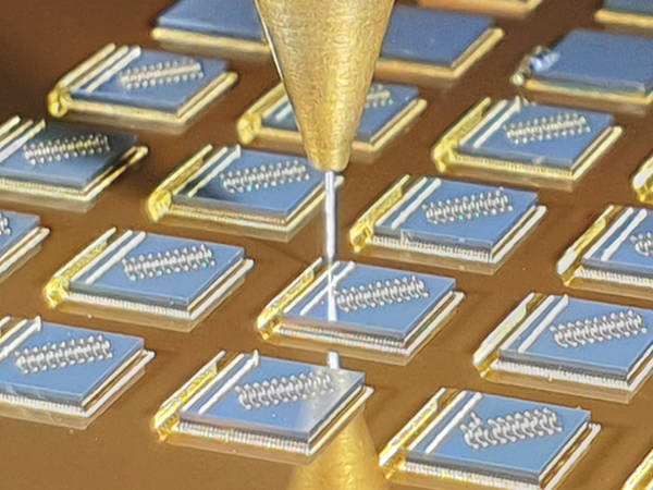
Semiconductors
- Element distributions one-, two- and three-dimensional
- Doping profiles, penetration depths and concentrations of dopants
- Surface impurities
- Layer sequences
- Diffusion lengths and constants of dopants for simulation tasks
- Barrier layers and their effect
- Adhesion of bonds (e.g. silicon-silicon wafer bonding, hydrophilic/hydrophobic)
- External sample analysis
- Surface defects
- Distribution of mechanical stresses in the semiconductor device
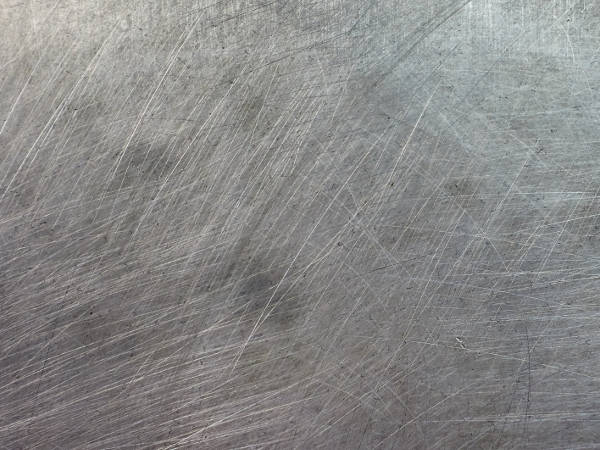
Metals
- Analysis of surface coatings
- Segregation within metallization layers
- Composition, thickness and sequence of layers
- Barrier layers and their effect
- Surface impurities
- Adhesion of adhesives, electroplated layer depositions and soldering
- Residual layer analysis
Glasses and insulators
- Surface coatings (e.g. lenses)
- Surface contamination
- Aging of surfaces
- Diffusion of network transducers
- Leaching processes in glasses
- Precipitate formation / crystallization processes
- Composition and layer thicknesses of insulator layer sequences
- Decorative and protective layers, adhesion promoters, …
- Delaminations
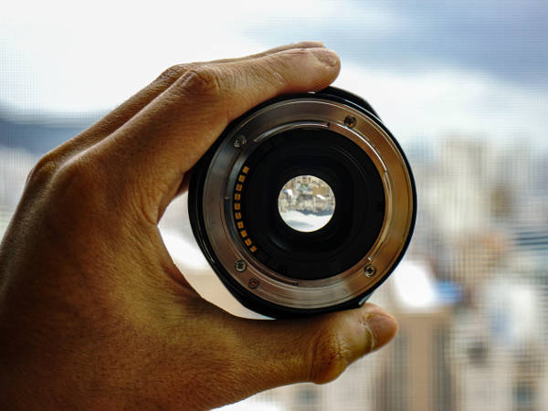
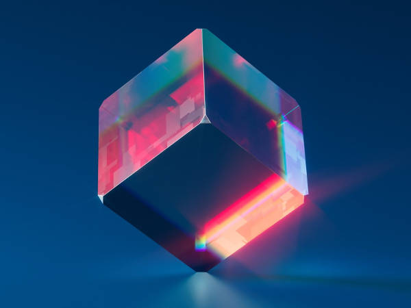
Optic
- Surface contamination
- Aging of surfaces
- Surface coatings (e.g. lenses)
- Reflective and anti-reflective coatings
- Filter layers (band-pass filters, UV-VIS-IR filters)
- Delaminations
Life Science
- Surface finishes
- Surface finish of implants
- Residual layer analysis
- Residue & particle analysis
- Dental fluoridation
- Environmental protection