The ever-growing market demand for highly stable and extremely accurate pressure sensors requires new ideas in addition to established solutions. The focus is primarily on reducing the cost of manufacturing components, integrating them into a higher level of integration, and calibration and testing. A prerequisite is a significant improvement in the ability to predict sensor performance in order to reduce development costs and development time.
In order to achieve high sensitivity in piezoresistive pressure sensors, silicon measuring resistors with low bordotation must be implemented. However, since these have a high temperature coefficient of resistance, the dependencies must be well known, measurable, and compensatable. To improve the sensor output signal, it is advantageous if the temperature dependence of the measuring resistors can be linearized.
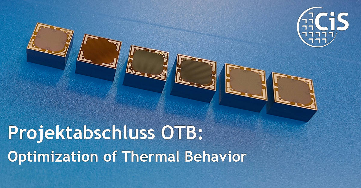
In the OTB project, scientists at the CiS Research Institute pursued the goal of reducing or optimizing the cross-sensitivity of highly stable and highly accurate piezoresistive resistance bridges consisting of resistance tracks implanted in single-crystal silicon with a high temperature coefficient. The investigations into the effect of technological and design measures focused on temperature ranges below freezing point and operating temperatures above approx. 80°C (up to 135°C), as stability is most critical in these ranges.
Various technological approaches were applied to a range of different chip designs. Various on-chip solutions for additional components were implemented and characterized, on the one hand to measure the chip temperature and on the other hand to compensate for differences in the bridge arms of the resistance bridge. Various resistive and bipolar components were adapted, manufactured, and analyzed for this purpose. Design rules for predicting temperature behavior were derived.
An alternative technological process was tested, which significantly improved the electrical isolation of the on-chip integrated temperature sensors from the measuring bridge. Two technological approaches were applied to the wafer production of 50 mbar sensor chips in the further development phase. Subsequently, new sensors were manufactured that are in direct bond contact with both thin and thick silicon backplates.
This revealed the specific advantages of each variant. For sensors of variant A, all project specifications regarding temperature dependence were met, whereas variant B with additional polysilicon resistors met the criterion of a voltage error reduction of less than 0.02% FS.
The results provide approaches for further metrological evaluations and improvements.
 The research and development work described was funded by the Federal Ministry for Economic Affairs and Climate Action (BMWK) as part of the Optimization of Thermal Behavior (OTB) research project.
Funding code: 49MF210191

