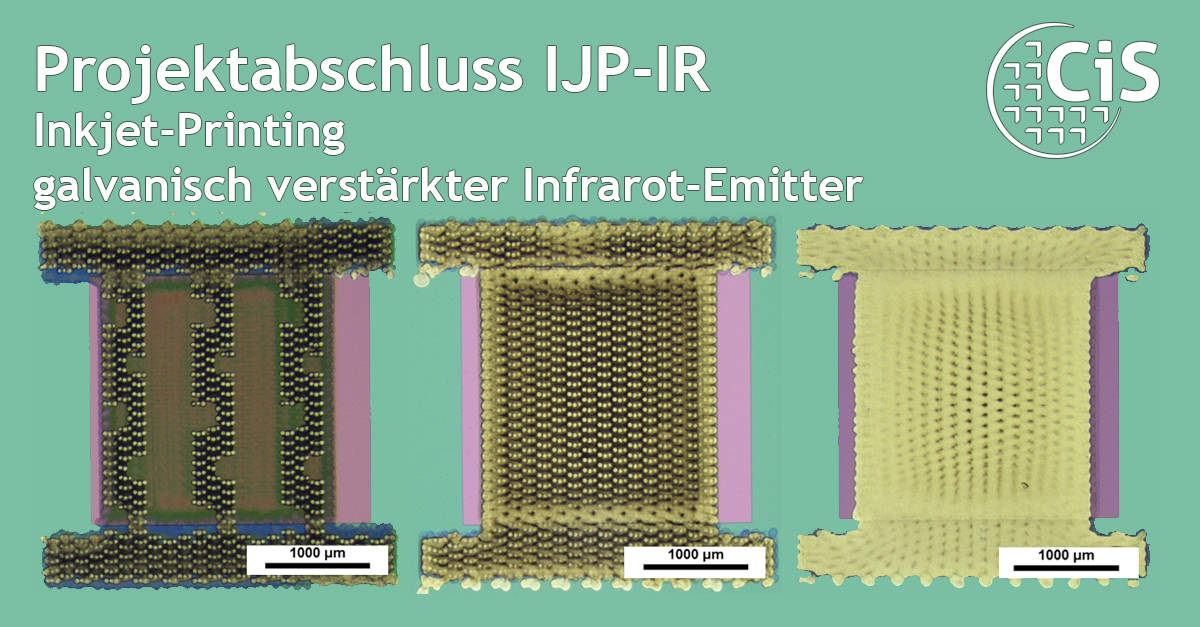
The increasing establishment of non-dispersive infrared (NDIR) sensor technology in the field of gas detection requires specific emitter and sensor systems for the respective application and its environmental conditions. A redesign of these IR emitters usually requires adjustments to the structure and the layer system. Traditional methods require time-consuming and costly process steps before a new prototype can be tested. In the completed IJP-IR research project, alternative processes based on inkjet technology and electroplating were therefore investigated for the manufacture of IR emitters. This new process reduces lithography and high-vacuum steps to a minimum and expands the material selection for CMOS-compatible systems. Based on in-house silicon-based layouts for infrared emitters, the first step was to convert an IR emitter layout into a bitmap format. This can be easily adapted in the software in a matter of minutes for the inkjet process and applied to the wafer via the printer without the otherwise necessary lithography and further etching steps. After printing, the conductivity of the printed layer and its adhesion to the silicon substrate were improved by means of a sintering process in a temperature range between 130 °C and 500 °C and a nitrogen atmosphere.
Further investigations then focused on galvanic processes. Here, additional metal layers such as copper were deposited on the printed silver layers. Regardless of the still immature adhesion between the silicon substrate and the printed and galvanic layers, the decisive advantage of this new process line clearly lies in the flexibility of the layout design and the materials to be applied.
 The research and development work described was funded by the German Federal Ministry for Economic Affairs and Energy (BMWE) as part of the research project “Inkjet Printing of Galvanically Amplified Infrared Emitters” (IJP-IR).
Funding code: 49VF123456

