27. March 2026
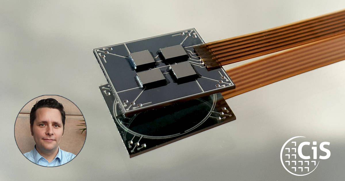
Dr. Martin Schädel, Head of the MOEMS departmenr at the CiS Research Institute, will discuss new possibilities offered by technologies for three-dimensional structuring of silicon in a webinar on Monday, 30th March 2026, at 15:00. In this one-hour Optica online seminar, following a brief overview of the technologies, he will use examples to illustrate the new functions that can be realized. These include, among others:
- tilted active surfaces used as light angle sensors
- free-form outer contours of the chip
- cavities in which light sources such as LEDs or lasers are integrated
- openings through which optical elements, fibers, or free beams can pass
- partially transparent photodiodes
Especially in combination with MEMS technologies, new functions and application-specific designs can be realized.
The webinar is aimed at engineers and scientists from development departments who already have a basic understanding of this topic.
» More information about the event organized by the Optica Technical Group

