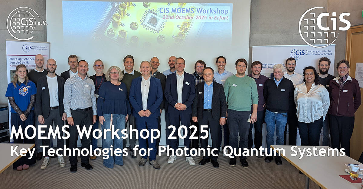
Under the motto “Key Technologies for Photonic Quantum Systems,” scientists and engineers from research and industry discussed the challenges and potential of photonic quantum technologies on 22nd October 2025. The MOEMS workshop in Erfurt was opened with a keynote speech by Dr. Robert Rölver (Q.ANT GmbH). Based on NV color center technology in diamonds, he vividly illustrated how a startup can be built from basic research into a company and demonstrated some possible applications. NV color centers are defects in the diamond lattice that can be used at room temperature and enable, for example, magnetometry for medical diagnostics, in which muscle signals are read as a human-machine interface for prosthetics.
This technological approach was explored in greater depth in Session 1: Dr. Robert Staake (Quantum Technologie GmbH) explained his development of a fully optical magnetic field sensor for use in harsh environmental conditions. Dr. Mario Bähr (CiS Research Institute) then discussed the challenges and solutions for the optical, mechanical, and electrical integration of diamond chips in quantum sensors and quantum computers.
Session 2 covered quantum cryptography and imaging. Dr. Alessandro Zanotti (Quantum Optics Jena GmbH) provided an overview of the development of hardware, software, and photonic systems as prerequisites for secure quantum communication. Building on this, Ms. Josefine Krause (Technical University of Munich) discussed the new QUICK3 project. The aim here is to ensure secure quantum communication with small satellites. In medical diagnostics, quantum mechanical effects are used, for example, to examine the behavior of living cells in a gentle imaging process. Dr. Frank Setzpfandt (FSU Jena/Fraunhofer IOF) reported on the challenges and possible solutions for future easy-to-use applications.
Session 3 dealt with photonic circuits for quantum applications: As an independent photonic design house based in the Netherlands, Dr. Jörn Epping (Epiphany Photonic Design House) presented possibilities for a comprehensive design flow up to the simulation of photonic circuits and layouts for a variety of materials, so-called PIC platforms. Dr. Jan Heine (Twin Photonics GmbH) spoke about turnkey integrated quantum light sources as a prerequisite for further innovations in quantum technologies, especially in imaging. Dr. Matthias Schmelz (Leibniz IPHT) dealt with the development of superconducting single-photon detectors (transition edge detectors, TES) for the VIS to NIR range. The contribution by Dr. Thomas Lisec (Fraunhofer ISIT) covered the application-specific production of micromagnets using the PowderMEMS process and potential applications for the miniaturization of quantum applications.
Session 4 concluded the workshop with enabling technologies for quantum technologies. Here, Dr. Indira Käpplinger (CiS Research Institute) addressed challenges and solutions for the integration of superconducting components for cryogenic application environments. Dr. Philipp Kellner (CiS Research Institute) introduced AsiSii defects in silicon as potential qubit candidates for quantum computing. Dr. Christian Zube (Veeco) presented the various manufacturing processes in the field of deposition and growth of extremely thin layers for quantum applications.
This year’s CiS MOEMS workshop offered all participants an excellent platform to intensively discuss findings from projects and industry, exchange experiences, and generate new ideas.

