The aim of the preliminary research project was to develop a robust, electrically readable sensor for determining layer stresses and film forces in thin layers in the range from approximately 1 N/m down to the mN/m and µN/m range. Thin functional layers are of central importance in semiconductor and MEMS processes, galvanic and chemical coatings, optical layers, and biosensor technology. Their mechanical stress is a decisive quality and process parameter. Established optically read cantilever systems achieve high sensitivity, but are sensitive to flow, difficult to control in electrolytes, and require complex equipment.
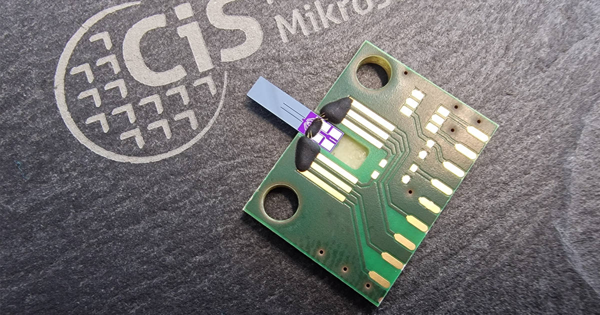
In the successfully completed project of the CiS Research Institute, a sensor concept based on piezoresistive bending elements was pursued. Three different layouts were investigated. Technologically, the structures were realized using CMOS-compatible processes: ion implantation for supply lines and measuring resistors, guard planes, deep etching to adjust the beam or membrane thickness, exposure of the bending elements, and assembly on test carriers or TO sockets.
The research results showed that the bending beam clamped on both sides was the preferred structure, offering high sensitivity, good handling, and significantly reduced cross-sensitivity to fluid flows. An ultra-thin bending plate, on the other hand, is particularly suitable for highly sensitive dynamic measurements down to the µN/m range. This provides a technologically compatible sensor concept that significantly expands the spectrum of film force-based sensor technology in thin-film technology, biosensor technology, chemical sensor technology, and in-situ process monitoring.
 The research and development work described was funded by the German Federal Ministry for Economic Affairs and Energy (BMWE) as part of the “Nanolever” research project.
Funding code: 49VF220011

