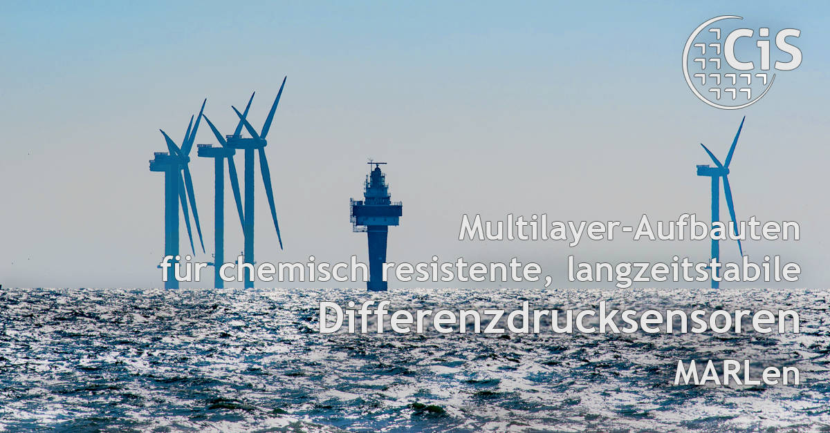
A typical example of a corrosive and at the same time electrically conductive medium is water. The oil, gas or offshore industry also has harsh measuring conditions. For monitoring and increasing efficiency, correspondingly cost-effective and application-specific differential pressure transmitters are required.
The approach pursued by the CiS Research Institute uses silicon as bulk material of components for front and back encapsulation of the finished components. With the further development of the existing wafer level packaging technologies, an idea was developed which dispenses with costly measuring cell concepts with stainless steel separating diaphragm and oil reservoir.
One solution approach was the targeted modification of the surface properties of typical MEMS silicon wafers with the primary goal of smoothing in the atomic range.
High strength was achieved by anodic Si-Si bonding with a thin, vapour-deposited borosilicate glass layer as well as with a screen-printed glass frit layer.
A differential pressure sensor demonstrator, in which the piezoresistive measuring bridge is completely encapsulated in the bulk silicon, with the option of additional passivation of all surfaces in contact with the media, served to prove the functionality. By means of implanted through-plating through a thin silicon layer, the chip metallization was completely separated from both media spaces.
All prototypes comply with the formulated requirements regarding sensitivity, overload resistance and long-term stability.
The solution approach for the media-resistant differential pressure sensor culminated in the German patent application entitled “Semiconductor-based differential pressure sensor and method for its manufacture” DE 10 2019 135 606.7.
 The research and development work described was funded by the Federal Ministry of Economics and Energy (BMWi) in the research project “Multilayer structures for chemically resistant, long-term stable differential pressure sensors” (MARLen).


