Impurities can be intentionally introduced into synthetic diamond in the form of nitrogen imperfections (“NV centers”). These have a spectrum of fascinating properties and open up the possibilities of using them for sensing. NV centers are optically active and are therefore also called color centers. With the help of these NV centers, physical effects can be observed even at room temperature that can only be described by quantum physical approaches. In addition, the state of the NV centers can be optically stimulated and read out.
NV centers in diamond crystal already gained widespread acceptance in the field of quantum sensing. However, real sensor elements based on NV centers for industrial applications have so far been available on the market at most as prototypes. The reasons for this are complex.
(1) Diamond material properties and availability:
Diamond with NV centers as an essential sensor component is offered by only a few commercial suppliers. These are limited in geometries, often have unattractive prices and long delivery times. In many cases, it is also unclear which specific material parameters in diamond are relevant at all. These include, for example, the density of NV centers and correlated quantities such as coherence times, but also other impurities.
(2) Sensor properties:
Optically addressing and reading out NV centers in diamond has already been demonstrated by a large number of scientific publications and does not represent a particularly high technical requirement. In addition to the diamond material with NV centers, a laser pointer, a filter and a photodiode are basically sufficient. To design and build a sensor that measures specific physical quantities (e.g. magnetism and linked electrical current density, temperature, mechanical pressure) in a reproducible qualitative and quantitative way, however, is challenging. Especially when miniaturized sensor assemblies are of interest, manufactured with industrially available processes.
(3) Linking diamond material and sensor properties:
Due to the diversity of possible applications in the field of sensor technology alone, a generalization of diamond material properties according to the motto “a lot helps a lot” is not practicable. For example, it is necessary to consider which sensory volume is required: A large volume contains a larger number of NV centers, which increases the fluorescence signal strength and thus the signal-to-noise ratio, but at the cost of lower lateral resolution. More cost-efficient diamond materials such as industrially produced HPHT diamond crystals offer high NV densities, but are not homogeneously doped locally, in contrast to such diamond films grown from the gas phase. Application-specific optimization of diamond materials to the desired sensor property must be performed.
These reasons (1)…(3) exemplify the problem that new materials have to enter the market: Pioneers -consortia from industry and academia- are needed to test diamond materials with respect to material properties, processability or application scenarios and thus also work towards a cost-attractive product. In DiaQuantFab, work with precisely this objective has been successfully carried out: Different diamond materials have been tested across the entire process chain, diamond has been specifically manipulated in properties such as NV density and used in specific demonstrators. These developments were accompanied by extensive characterizations and the development of measurement methods.
One of these applications was the determination of magnetic fields: Changing the spin state of NV centers by an external magnetic field changes their fluorescence signal. This can be used to infer the strength of the external magnetic field or, in direct correlation, a current strength. Three demonstrators were (further) developed for industrially relevant applications: One magnetic field sensor system each for position sensing and atomic force microscopy, as well as an ammeter based on a similar functional principle.
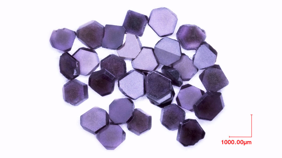
- As a result of the project, the following were developed, among others,a high throughput processing method for industrially fabricated single crystal HPHT diamond materials having high NV density, {111} orientation and cost potential <4 €,
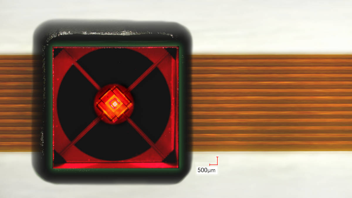
- an industrializable miniaturized emitter-receiver unit with integrated diamond plate suitable for sensitive magnetic field measurements in zero field and as an ammeter with an edge length of 10×10 mm²,
- a position sensor for the readout of magnetically coded scale tapes with two or four channels,
- thin CVD-synthesized diamond films with NV centers in only one crystal orientation,
- the development of methods for the stabilization of NV centers with the help of charges.
As a result of DiaQuantFab, cost-efficient diamond material is to be brought to market, and further bilateral and also publicly funded research projects are to be initiated. It will be interesting to see whether the insights gained into the opportunities and limitations of quantum technology will lead to further new product ideas and developments among the industrial partners.
The partners:
- Balluff GmbH (Neuhausen a.d.F.): Sensor and automation specialist
- CiS Forschungsinstitut für Mikrosensorik (Erfurt): Si-based sensor technology & research transfer
- Diamond Materials GmbH (Freiburg i.Brsg.): High Purity CVD Diamond Disc Manufacturer
- nano analytik GmbH (Ilmenau): Manufacturer of various scanning probe technologies
- Universität Leipzig (Prof. J. Meijer): Solid state physics, manipulation of diamond
- Universität Stuttgart (Prof. J. Wrachtrup): 3rd physics institute, NV-based sensor technology
- Universität Ulm (Prof. F. Jelezko): Quantum optics and diamond growth
The coordinator for the project was the CiS Research Institute.
About the joint project:
Over a period of three and a half years, the project team in the BMBF joint project “DiaQuantFab” investigated diamond materials for industrial applications and developed optical microsensor systems based on NV centers in diamond. The project ended on November 30, 2022, taking a holistic approach along the value chain from diamond production and manipulation to the finished sensor system. The selected sensor systems were magnetic field sensors for the application areas of position measurement technology, scanning probe microscopy and current measurement. The project consortium included Balluff GmbH (Neuhausen a.d.F.), Diamond Materials GmbH (Freiburg i.Brsg.), nano analytik GmbH (Ilmenau), University of Leipzig (Prof. J. Meijer), University of Stuttgart (Prof. J. Wrachtrup), University of Ulm (Prof. F. Jelezko) as well as the CiS Research Institute for Microsensors (Erfurt), through which the joint project was also coordinated.
Funded by
 The joint project “DiaQuantFab – Standardization in the production and processing of quantum materials using the example of NV color centers in diamond for the realization of a high-precision ammeter based on quantum effects” was selected for funding by the German Federal Ministry of Education and Research (BMBF) in the call “Key Technologies for Quantum Sensor Technology”.
Funding code: 13N14984
HPHT diamond platelets with high NV density, thickness approx. 300 µm
Miniaturized emitter-receiver unit with integrated diamond, as sensitive zero-field magnetometer or ammeter
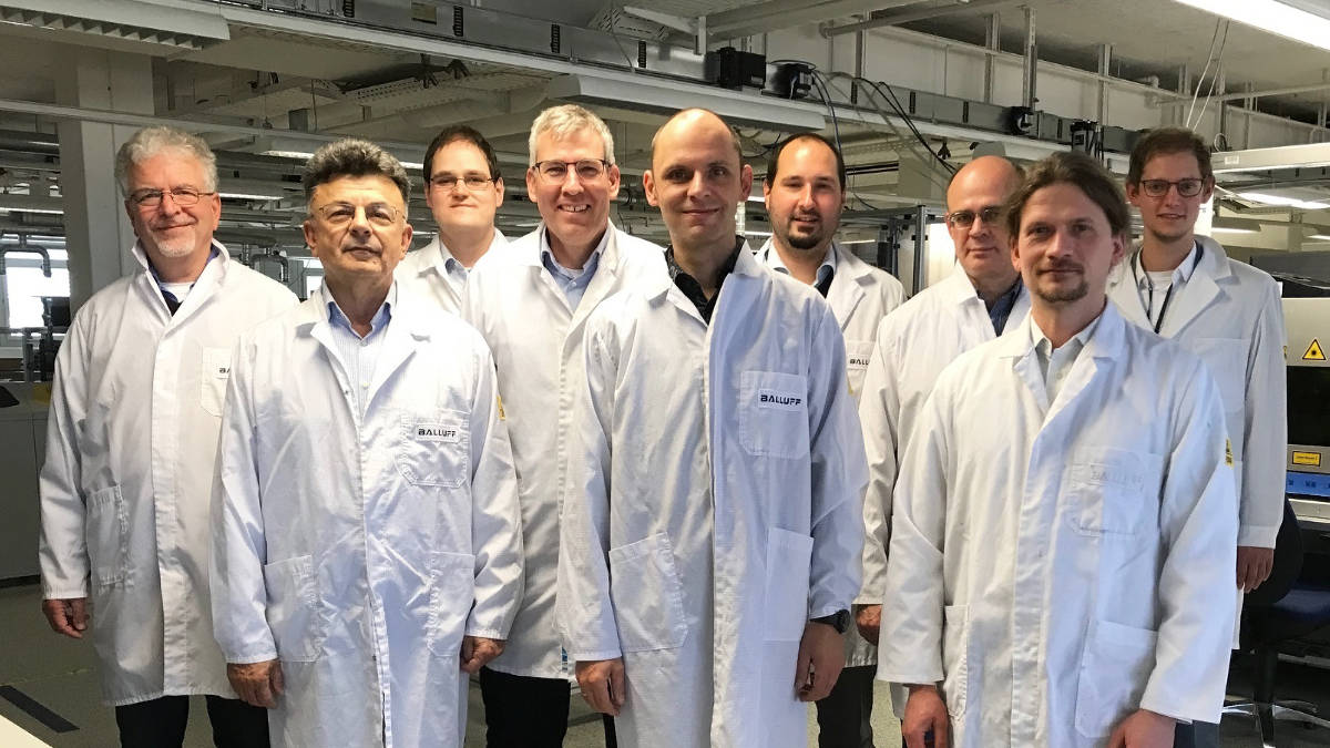
Hybrid conducted final meeting, held at Balluff GmbH
Online participants of the hybrid final meeting
Partner in the joint project


