
Highlight of the CiS Forschungsinstitut at the Hannover Messe 2024: Galvanically isolated incremental sensor
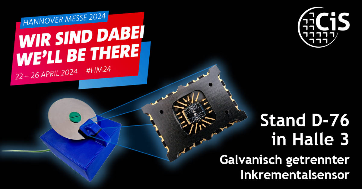
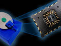
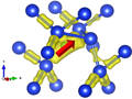
During the Hannover Messe, which starts next week, the CiS Research Institute will be presenting an electrically isolated incremental sensor at the joint Thuringian stand in Hall 3, Stand D76. As part of the “GalGiS” funding project, new silicon technologies were developed to achieve such galvanic isolation at chip level.
Photodiode arrays with an integrated LED light source were developed as demonstrators, which achieve high dielectric strengths (up to 1500 V) at a distance of just 150 µm between the elements. The new technology guarantees the usual geometric accuracy in the sub-micrometer range. As a result, high-precision phase positions and signal ratios are realized reproducibly and with long-term stability and application-specific requirements are achieved.
The galvanic incremental sensor can be used in optical encoders for position and speed sensors – especially where high technical safety is required – for example in aerospace, rail transportation and medical technology.
» Infosheet: Galvanically isolated incremental sensor (GalGIS)
Infrared emitters with dynamic range greater than 100 Hz
Infrared MEMS emitters are powerful alternatives to classic light bulbs. These heat emitters can cover the spectral range from 2 to 15 µm and achieve dynamic modulations of up to 30 Hz. A recent development has even pushed the dynamic range beyond the 100 Hz limit.
One application for the fast infrared emitter array is in non-dispersive infrared spectroscopy (NDIR) for gas detection and concentration for medical and industrial applications.
» Infosheet: Fast infrared emitter array (FIRE)
Avalanche photodiode with enhanced blue and ultraviolet amplification
APDs are often used for the detection of weak light. Standard APDs have a peak sensitivity at wavelengths > 500 nm. The new BV-APD developed achieves excellent performance for UV and blue light with a spectral range of 250-700 nm and can be customized.
» Infosheet: Highly sensitive low-noise blue-violet avalanche photodiodes (BVAPD)
In addition to the portfolio of photodiodes, the CiS Research Institute will also be showing a selection of MEMS developments. These include:
» Infosheet: High-end acceleration sensors (HEB)
» Infosheet: Hybrid silicon strain sensors (SiDMeses)
» Infosheet: Retrofit kit for non-invasive pressure measurement (NivLer)
 The research and development work described in the following research projects was funded by the Federal Ministry of Economic Affairs and Climate Action (BMWK):
Galvanically isolated incremental sensor (GalGIS)
Funding code: 49VF123456
Fast infrared emitter array (FIRE)
Funding code: 49MF220020
Highly sensitive low-noise blue-violet avalanche photodiodes (BVAPD)
Funding code: 49MF200098
High-end acceleration sensors (HEB)
Funding code: 49VF200064
Improving the stability of hybrid silicon strain sensors (SiDMeses)
Funding code: 49MF200061
Retrofit kit for non-invasive pressure measurement (NivLer)
Funding code: 49MF220174

Packaging technology for thermal flow sensors
The newly launched Pack-Flu project deals with the design, realization and characterization of a robust and innovative packaging platform for low-cost MEMS-based microcalorimetric flow sensors for use in gas pipelines or ventilation systems. The platform serves as a scalable basis for flow sensors for analyzing and controlling air flow, hydrogen and other non-aggressive gases with known flow direction (e.g. in pipelines) with high accuracy
MEMS Pirani sensor for fine and high vacuum
With the MinerVa project, the CiS Research Institute is launching the development of a MEMS Pirani sensor for pressure measurement in the fine high vacuum range. The potential applications are diverse, for example in the production of thin functional layers using physical vapor deposition (PVD)

Happy Easter – Creative competition for the children of our employees
Once again this year, the management of the CiS Research Institute invited employees to take part in a creative hands-on activity during the Easter period. The children of all employees were invited to submit self-drawn pictures of the Easter bunny or Easter crafts by today. Each participating child received a sweet surprise as a reward. The numerous creative submissions from the young artists can be admired in our online gallery.
High-end acceleration sensors
The project dealt with the development of capacitive accelerometers with a resolution of 0.001⁰ based on chip-level processes. The main features are a significantly increased seismic mass, a laterally arranged differential capacitor and a hermetic package

Photoacoustic gas sensors with reference gas sensor
The focus of the completed PAS research project was the development of a piezoresistive microphone component based on micromechanical systems (MEMS) for highly integrated photoacoustic gas sensors. The sensor is suitable for an application range from -40⁰C to 140⁰C. Applications are in the field of climate and environmental protection to improve energy management, air quality testing or in medical technology as highly sensitive breathing gas sensors.
Defect mechanisms in silicon – Lectures at the DPG Spring Conference in Berlin
From 17th-22nd March 2024, the Sektion Kondensierte Materie (SMK) of the Deutsche Physikalische Gesellschaft e. V. (DPG) together with its specialist associations and working groups is organizing the DPG Spring Conference on the campus of the Technical University of Berlin. In four contributions, Dr. Kevin Lauer and young researchers will present their latest scientific results on various defect mechanisms in silicon at different doping levels and invite discussion

Evaluation of quantum materials in industrial pressure sensors
At the CiS Research Institute, pressure sensors based on NV centers in diamond were produced using industrial manufacturing methods in cooperation with partners from industry and science. The results of the Qind research project will be presented at the 28th Hasselt Diamond Workshop SBDD
Innovative isothermal sensor with front cavities
In the completed NIVo research project, a new thermopile sensor was developed that works on the principle of isothermal detection of infrared radiation and is exempt from the front side. This combination enables the production of a new type of high-performance sensor in the field of thermography

Member meeting OptoNet Live – The CiS Research Institute introduces itself
As a long-standing member of OptoNet e.V., we are taking the opportunity to introduce ourselves to the members of the Photonics Network Thuringia at the virtual members’ meeting on Monday, 19th February 2024. Dr. Martin Schädel, Head of Business Unit MOEMS, will present the institute as a partner for production-oriented research and development of new sensor solutions and microsystems based on silicon technologies