CiS
  • Research Institute
    • Profile
    • Certification
    • Network
    • Downloads
  • Competences
    • Technologies
    • Simulation & Design
    • Process Development
    • Wafer Processing
    • Assembly & Packaging
    • Measurement & Analytics
    • CAK – CiS Analytics Comptence Center
    • Prototyping & Small Batches
  • R&D
    • Microsensors for the World of Tomorrow
    • MEMS
    • MOEMS
    • Public Research
    • Funding
    • Industry Projects
  • Markets
    • Applications
    • Process measurement technology
    • Energy
    • Mobilty
    • Health
    • Climate
    • Infrared sensor technology
  • Career
    • Working in the Research Environment
    • Staff
    • Students
    • Training
    • Privacy Policy on Applications
  • News
    • News
    • Events
    • Publications & Conferences
  • CiS e.V.
    • The Association
    • Charter (PDF)
    • The Board
    • Contact CiS e.V.
    • Privacy Policy CiS e.V.
  • Contact
    • Contact Persons
    • Approach
    • Imprint
    • Privacy Policy
  • Deutsch
  • Click to open the search input field Click to open the search input field Search
  • Menu Menu

Project start DiaTip: Active diamond-based scanning probes for QUANTUM metrology and nanofabrication – development of hybrid assembly methods

You are here: Home1 / News2 / Project start DiaTip: Active diamond-based scanning probes for QUANTUM...
2. August 2023

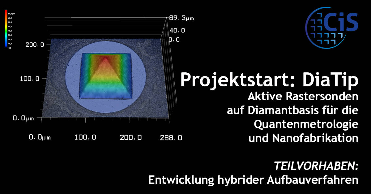
Future technologies in microelectronics, biotechnology, nanotechnology, medical technology, quantum technologies and single-atom process methods require the use of scanning probe microscopy (SPM). Scanning probes are micromechanical cantilevers that are used to characterize and manipulate a wide variety of material surfaces, in extreme cases at the atomic level. The CiS Forschungsinstitut für Mikrosensorik GmbH together with the company nano analytik, the TU Ilmenau as well as other associated industrial partners have set themselves the aim of developing a cost-efficient manufacturing process for diamond tips. These will be combined with active microcantilever technology (integrated piezoresistive readout and electro-thermo-mechanical actuation). The project also includes the development of an assembly process for joining the two components “active microcantilever” and “diamond tip in a pilot production”.

The special material properties of diamond allow the adjustment of different properties of the diamond tips: For example, on the one hand, a dimensionally stable hollow tip can be created due to its high hardness, which can also be equipped with high electrical conductivity. On the other hand, by introducing nitrogen defect centers (“NV centers”) and implementing optical components to excite these color centers and read out the fluorescence response of them, a magnetic field sensitive sensor can be created.

The scope of work covered by the CiS Research Institute is concerned with the development of a pilot production-ready process for the high-precision assembly of diamond tips on active microcantilevers, the simulation and optimization of the optical components, the fabrication of Si impression bodies for the cost-effective fabrication of diamond tips based on a MEMS process, and the fabrication of a cantilever with a photodiode.

The SME-innovative joint project “Active diamond-based scanning probes for QUANTUM metrology and nanofabrication (DiaTip) – sub-project development of hybrid assembly processes” is supported by the BMBF as part of the “SME-innovative” funding program.
Funding code: 13N16579

Categories:
  • Analytics
  • Automotive
  • CiS general
  • Digitalization
  • Energy
  • Events
  • Force
  • High Temperature
  • Hydrogen
  • Invest
  • IR
  • Jobs
  • Measurement
  • Medical technology
  • MEMS
  • MOEMS
  • Packaging
  • Personnel
  • Photonic
  • Politics
  • Pressure
  • Process development
  • Quantum
  • Silicon Detectors
  • Simulation & Design
  • UV
  • Waferprocessing
Project:
  • DiaTip
  • Share on Facebook
  • Share on X
  • Share on WhatsApp
  • Share on LinkedIn
  • Share by Mail
  • News
  • Events
  • Publications & Conferences
  • ISEC 2025 – Full Agenda with plenary speakers is available

    9. May 2025
  • CiS Research Institute at the international conference MATERIALSMEET2025 in Budapest

    2. April 2025
  • Visit us at the HANNOVER MESSE 2025

    25. March 2025
  • End of project PoRr: Photodiodes without back reflection

    20. March 2025
  • CoGeQ project meeting at the CiS Research Institute

    14. March 2025

Categories

  • Analytics (19)
  • Automotive (11)
  • CiS general (28)
  • Digitalization (1)
  • Energy (19)
  • Events (188)
  • Force (44)
  • High Temperature (1)
  • Hydrogen (2)
  • Invest (1)
  • IR (34)
  • Jobs (4)
  • Measurement (22)
  • Medical technology (83)
  • MEMS (157)
  • MOEMS (158)
  • Packaging (59)
  • Personnel (9)
  • Photonic (21)
  • Politics (22)
  • Pressure (59)
  • Process development (5)
  • Quantum (33)
  • Silicon Detectors (21)
  • Simulation & Design (22)
  • UV (28)
  • Waferprocessing (16)

Archives

From design to prototyping.
Reliable. Long-term stable. Precise.

Konrad-Zuse-Str. 14
99099 Erfurt
Germany

Tel.: +49 361 663 1410
E-Mail: info@cismst.de

© 2025 CiS Forschungsinstitut für Mikrosensorik GmbH
  • Start
  • Deutsch
  • Imprint
  • Privacy Policy
  • Sitemap
Link to: Novel material combinations and sensor geometries for resistance thermometers in the hydrogen economy Link to: Novel material combinations and sensor geometries for resistance thermometers in the hydrogen economy Novel material combinations and sensor geometries for resistance thermometers... Link to: Project start NivLer: Retrofit kit for non-invasive pressure measurement Link to: Project start NivLer: Retrofit kit for non-invasive pressure measurement Project start NivLer: Retrofit kit for non-invasive pressure measurement
Scroll to top Scroll to top Scroll to top