Also this year, three workshops on silicon-based sensor technology and related, current research results and latest trends within the individual focus topics will take place. The workshops will take place as a hybrid event in the large conference room at the CiS Research Institute in Erfurt. The organizer is CiS e.V.
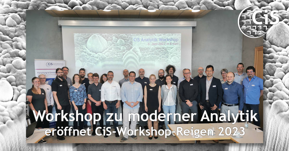
The first of these three workshops was themed “Modern Analytics for Innovative and Sustainable Sensor & Materials Science” and highlighted current results from research and development in modern analytics for the semiconductor industry on June 6, 2023. The development of sophisticated new sensors and materials always requires a precise understanding of the material or component surfaces. What is the physical and chemical nature of the component, how does it change through use, what about environmental compatibility or the quality and control of underlying manufacturing processes? Surface analysis provides the answers to these questions.
In the hybrid workshop, various methods of surface analysis and other special procedures were presented and their applications and potential were demonstrated using current examples from research and development. The workshop was introduced by Prof. Christoph Gerhardt from HAWK Göttingen with the lecture “Calibration-free investigation using laser-induced plasma spectroscopy (LIBS) for the quantification of trace elements in glasses”.
One focus of the workshop was the analysis of materials by secondary mass spectroscopy (SIMS), which is available at the CiS Research Institute. After a short introduction, Dr. Stefanie Reiß, responsible for SIMS at the CiS Research Institute, explained investigation results for quantum technological applications. Here, the main focus was on the investigation of defects in the diamond crystal lattice and their effects. SIMS is, for example, one of the most powerful analytical methods for the precise determination of very low nitrogen concentrations in diamonds.
In his presentation “10 years of ASi-Sii defect”, Dr. Kevin Lauer from the CiS Research Institute discussed the analytical breakthroughs that have contributed significantly to the understanding of this defect category in silicon devices.
The company nano analytik GmbH presented the initial results of its cooperation with the CiS Research Institute, which were developed as part of the two BMBF-funded cooperation projects “DiaQuantFab” and “DiaTip”.
Guided tours of the Analytics Competence Center at the CiS Research Institute accompanied the workshop and contributed to a lively exchange of ideas and experiences.
Two more workshops are planned for the fall. On 12th September 2023, the Assembly and Packaging Workshop will focus on current developments in hybrid and wafer-level assembly. The Simulation and Design Workshop on 26th September 2023, will focus on modeling in microsystems technology. Individual slots are still available and registrations are already possible.
 The joint project “DiaQuantFab – Standardizations in the production and processing of quantum materials using the example of NV color centers in diamond for the realization of a high-precision ammeter based on quantum effects” was selected for funding by the German Federal Ministry of Education and Research (BMBF) in the call “Key Technologies for Quantum Sensor Technology”.
Funding code: 13N14984
 The joint project “DiaTip – Active diamond-based scanning probes for QUANTUM METROLOGY and nanofabrication (DiaTip) – Subproject: Development of hybrid assembly processes” was selected for funding by the German Federal Ministry of Education and Research (BMBF) in the call “KMU-innovativ- Verbundprojekt”.
Funding code: 13N16579
