
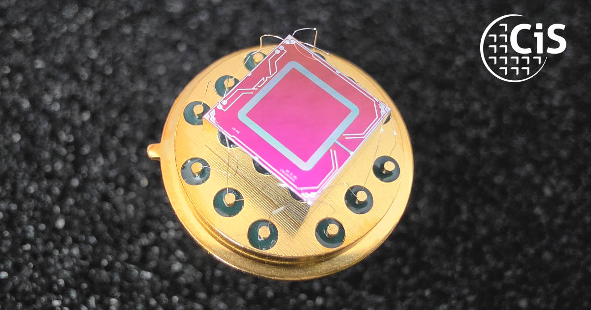
MEMS-based sensor systems often utilize the piezoresistive effect, a principle that is highly sensitive to pressure and force. A common problem is the almost always present zero-offset signal and its strong temperature dependence (TCO, temperature coefficient of offset). This can compromise the accuracy and stability of measurements and ultimately have a negative impact on performance. The completed “miniOffset” project therefore aimed to develop a scalable platform in which these two parameters can be virtually eliminated at the wafer or chip level.
Through simulations, various designs were selected and fabricated, and a robust chip design was created.
In conjunction with this design, extensive technology optimization was carried out, and various approaches were tested. The most efficient approach was the integration of various offset structures – such as microfuses for burning through and small resistors for switching on and off – into a measuring bridge.
An approach to minimizing the offset was achieved for chip variants with large offset deviations and variations through the use of stud bumping on offset structures (Fig. (a)). This method utilizes the offset structures, consisting of various resistors that are spatially separated from one another. First, the offset voltages of the investigated wafers are measured again. Subsequently, a program (Python) was created that reads in the offset values, calculates the resistance difference required to minimize the offset, and outputs the resistors to be short-circuited via stud bumping. Figs. (b) and (c) show example results from a wafer with 90 chips.
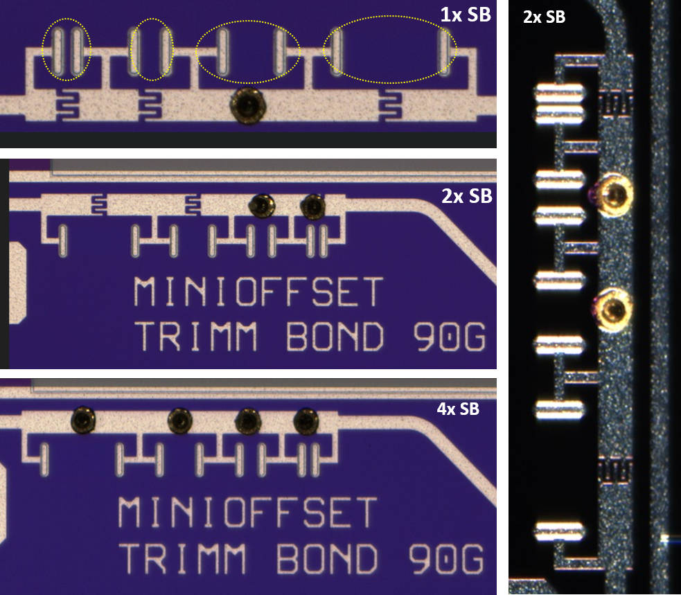
(a) Offset structures consisting of 7.5 Ω, 15 Ω, 30 Ω, and 60 Ω resistors, including the mounted stud bumps
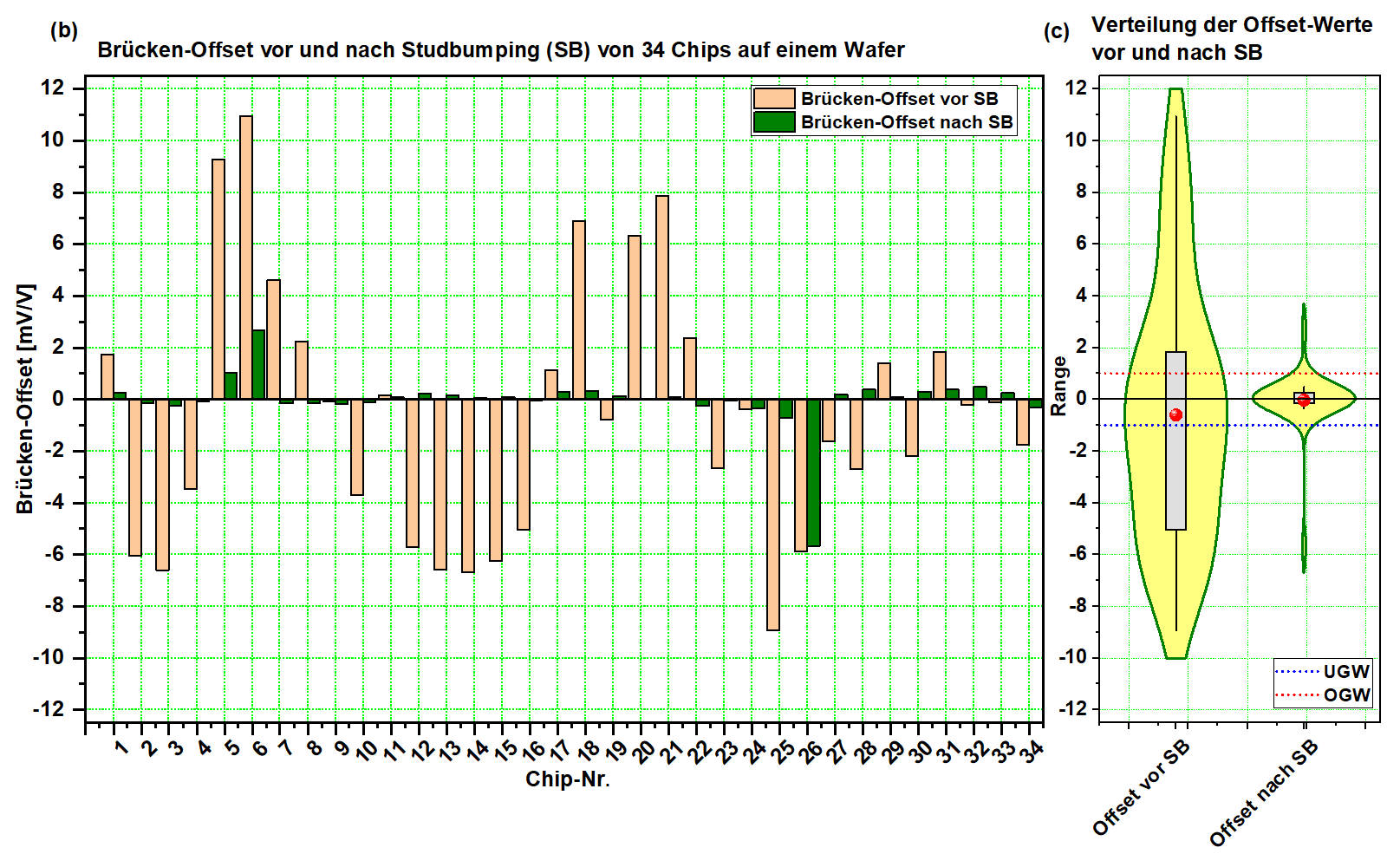
(b) Offset values and a chip variant VII with the greatest variation and deviation, and (c) their distribution, before and after offset correction using stud bumping
As can be seen in the graph, this method was able to significantly reduce the majority of offset values and, for most chips, even correct them to nearly zero. These results indicate that this method is suitable for correcting deviations from initial offset values. It can also be cost-effectively integrated into the manufacturing process, since wire bonding – the process used to correct the offset values of individual chips – is already part of the sensor manufacturing process.
» Infosheet: Piezoresistive Technology Platform with Minimal Offset (PDF)
 The research and development work described here was funded by the Federal Ministry for Economic Affairs and Energy (BMWE) as part of the research project “Piezoresistive Technology Platform with Minimal Offset” (miniOffset).
Funding code: 49MF220087