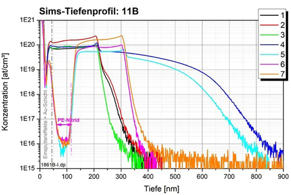
Conventional radiation detectors involve pn-junction formation, diffusion, or implantation steps during manufacturing. This creates a direct connection between the high-purity substrate region and the highly doped silicon. This interface is often riddled with crystal defects and is frequently a major cause of high dark currents in the detector. In the preliminary research project, the structure of the pn junction was redesigned: The p-type and n-type regions were completely separated, thereby reducing the transition zone and significantly lowering the dark current. To achieve this, a tunnel or barrier oxide was successfully grown on the silicon, followed by an additional layer of highly doped polysilicon. This created a passivation layer that also serves as an electrical contact. This architecture is known in photovoltaics as TOPCon technology – but had not previously been used for detectors.
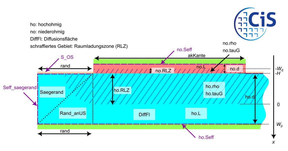
In parallel, the causes of reverse-bias dark currents in abrupt pn junctions were investigated. The current paths were modeled as one-dimensional boundary value problems and solved analytically. This approach allows complex structures to be reduced to simpler, one-dimensional boundary value problems and forms the basis for a future behavioral model capable of predicting the I-V characteristics of radiation detectors and photodiodes in both the forward and reverse directions. Furthermore, the research results obtained contribute to a deeper understanding of new passivation technologies and are a prerequisite for the development of more powerful radiation detectors in medical technology (X-ray imaging, radiation therapy, dosimetry), environmental sensor technology (measurement of ionizing radiation), and nuclear research (DESY, CERN).
 The research and development work described here was funded by the Federal Ministry for Economic Affairs and Energy (BMWE) as part of the research project “Innovative Oxide Structures for the Passivation of Silicon Interfaces” (InOxA).
Funding code: 49VF220049